Lam Research: A Key Enabler of Next-Gen Semiconductors
Advanced Deposition and Etch Technologies Powering Chip Miniaturization

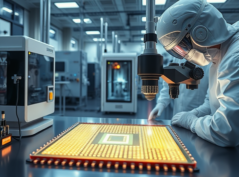
As the demand for faster, smaller, and more energy-efficient electronic devices continues to grow, the semiconductor industry faces the challenge of pushing the limits of Moore’s Law. Lam Research plays a critical role in enabling this progress through its cutting-edge deposition and etch technologies, which are essential for manufacturing next-generation chips.
Deposition and etching are two fundamental processes in semiconductor fabrication. Deposition involves layering materials onto a silicon wafer, while etching selectively removes those materials to create intricate patterns that define a chip’s functionality. As transistors shrink to the nanoscale, precision and uniformity in these processes become increasingly vital.
Lam Research has pioneered atomic layer deposition (ALD) and atomic layer etching (ALE), which allow for angstrom-level control over material placement and removal. These techniques are key to achieving the extreme aspect ratios and tight tolerances required for advanced nodes, such as 3nm and beyond. By enabling more precise patterning, Lam’s technologies help increase transistor density, reduce power consumption, and improve overall chip performance.
Moreover, Lam’s innovations support the integration of new materials, such as high-k dielectrics and metal gates, which are essential for maintaining performance at smaller geometries. Their equipment also enables 3D architectures like FinFETs and gate-all-around (GAA) transistors, which are becoming standard in cutting-edge designs.
For engineers, designers, and tech companies, understanding these technologies is crucial. They not only drive the capabilities of smartphones, data centers, and AI systems but also shape the future of computing. Lam Research’s work ensures that the semiconductor roadmap remains on track, making powerful, compact, and efficient electronics possible.
For more technical insights, you can explore Lam Research’s official technology page: https://www.lamresearch.com/technology/
Surface Refinement Processes that Ensure Atomic-Level Accuracy

In the race to develop next-generation semiconductors, achieving atomic-level precision in surface refinement is not just a technical feat—it’s a necessity. Lam Research, a global leader in semiconductor manufacturing equipment, plays a pivotal role in this process by enabling ultra-precise surface engineering through advanced plasma etching and atomic layer deposition (ALD) technologies.
At the heart of modern chip fabrication lies the need to manipulate materials at the atomic scale. As transistor sizes shrink below 5nm and even approach the angstrom level, any surface irregularity can lead to performance degradation or device failure. Lam’s surface refinement processes are designed to ensure that every layer deposited or etched meets the strictest uniformity and precision standards.
One of the key technologies Lam utilizes is Atomic Layer Etching (ALE), which allows for the controlled removal of material one atomic layer at a time. This method ensures minimal damage to underlying layers and provides unmatched selectivity, crucial for maintaining the integrity of increasingly complex 3D structures like FinFETs and Gate-All-Around (GAA) transistors.
In tandem, Atomic Layer Deposition (ALD) is used to deposit ultra-thin films with atomic-level control over thickness and composition. This is essential for forming high-k dielectrics and barrier layers that are both uniform and defect-free, enabling higher performance and lower power consumption in chips.
Lam Research’s innovations in surface refinement are not only advancing Moore’s Law but also supporting the broader semiconductor ecosystem in delivering more powerful, energy-efficient, and compact devices. These advancements directly impact our daily lives—from faster smartphones to more capable AI processors and energy-efficient data centers.
For more technical insights, you can visit Lam Research’s official technology blog: https://blog.lamresearch.com
Advanced Deposition and Etch Technologies Powering Chip Miniaturization

As the demand for faster, smaller, and more energy-efficient chips continues to rise—especially with the explosive growth of AI, 3D NAND, and advanced logic devices—Lam Research plays a pivotal role in enabling these innovations. At the heart of this transformation are Lam’s cutting-edge deposition and etch technologies, which are essential for manufacturing next-generation semiconductors.
Deposition and etching are two of the most critical steps in semiconductor fabrication. Deposition involves layering materials atom by atom, while etching removes specific layers with extreme precision. Lam’s advanced atomic layer deposition (ALD) and atomic layer etching (ALE) tools allow chipmakers to build structures at the nanoscale, supporting the production of transistors with gate lengths under 5nm.
For AI chips, which require dense and high-performance architectures, Lam’s technology enables precise patterning and scaling of logic transistors. In 3D NAND, where memory cells are stacked vertically, Lam’s etch tools help achieve deep, narrow trenches with uniform profiles—critical for increasing storage capacity without expanding chip size.
Moreover, Lam’s innovations in selective etching and high-aspect-ratio deposition are helping to overcome the physical limitations of Moore’s Law. These breakthroughs not only enhance performance but also reduce power consumption, making devices more sustainable and efficient.
Lam’s contributions are not just technical—they’re transformative. By enabling the production of smaller, faster, and smarter chips, Lam is accelerating advancements in AI, mobile computing, data centers, and beyond.
For a deeper dive into Lam’s technology and its impact on the semiconductor industry, you can visit their official site: https://www.lamresearch.com
Global Market Influence, Financial Strength, and Competitive Edge

Lam Research plays a pivotal role in the global semiconductor industry, not just as a technology provider but as a strategic enabler of next-generation chip innovation. Its influence extends across three key pillars: global market presence, robust financial health, and a strong competitive edge.
First, Lam Research’s global market influence is substantial. With operations in over 16 countries and partnerships with leading semiconductor manufacturers, Lam supports the production of advanced chips used in smartphones, data centers, AI systems, and automotive electronics. Its tools are essential for atomic-level precision in etching and deposition processes, which are critical for producing smaller, more powerful chips.
Second, the company’s financial strength provides it with the resilience and flexibility to invest in R&D and weather industry cycles. In fiscal year 2023, Lam reported revenues exceeding $17 billion, demonstrating strong demand for its products and services. Its consistent profitability and solid balance sheet allow for continuous innovation and strategic acquisitions that reinforce its market position.
Lastly, Lam’s competitive edge lies in its advanced technology portfolio and customer-centric approach. The company is a leader in high-aspect-ratio etching and atomic layer deposition—technologies that are crucial for 3D NAND and advanced logic chips. Lam also works closely with customers to co-develop solutions tailored to future node requirements, giving it a collaborative advantage in a rapidly evolving industry.
In a world increasingly driven by semiconductors, Lam Research’s influence is both foundational and forward-looking. For those interested in the broader semiconductor ecosystem, understanding Lam’s role offers valuable insight into the forces shaping our digital future.
For more information, you can visit Lam Research’s official investor relations page: https://investor.lamresearch.com/