Applied Materials and Chipmaking: The Pickaxe Power Behind Semiconductor Innovation
Market Leadership in the Semiconductor Equipment Industry
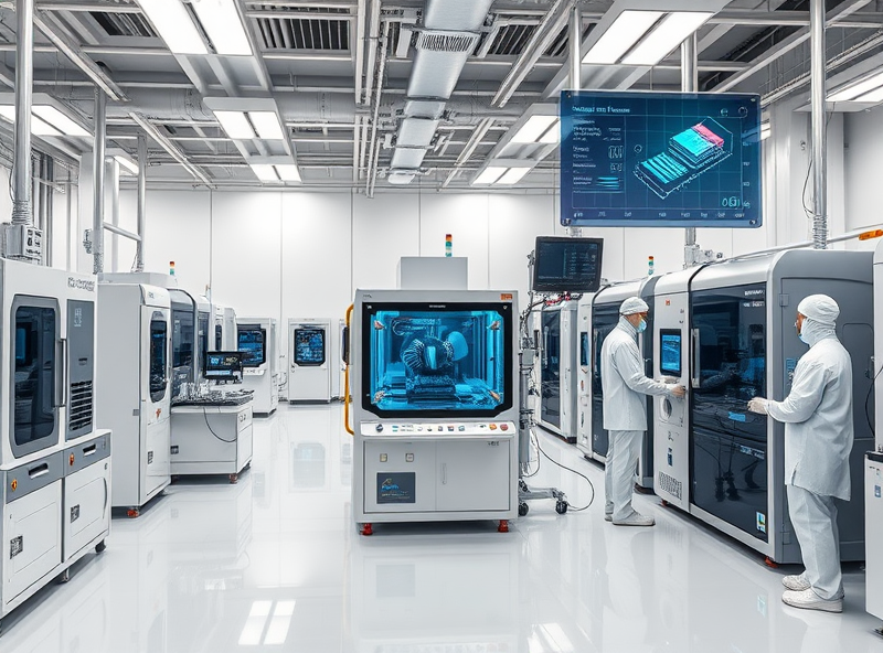
In the ever-evolving world of semiconductor manufacturing, Applied Materials stands as a pivotal player—often referred to as the ‘pickaxe supplier’ in the gold rush of chip innovation. While tech giants like Intel, TSMC, and Samsung dominate headlines, it’s companies like Applied Materials that quietly enable their success by providing the essential tools and technologies for chip fabrication.
Applied Materials leads the semiconductor equipment industry by offering advanced deposition, patterning, and inspection systems that are crucial for producing next-generation chips. Their innovations in atomic layer deposition (ALD), chemical vapor deposition (CVD), and etching processes allow chipmakers to build smaller, faster, and more energy-efficient semiconductors. This leadership is not just about market share—it’s about being at the forefront of enabling Moore’s Law to continue.
One of the key reasons for Applied Materials’ market dominance is its strong investment in R&D. In 2023 alone, the company invested over $2.7 billion in research and development, focusing on new materials and 3D architectures that are essential for AI, 5G, and high-performance computing. This commitment ensures that their tools remain indispensable as chip complexity increases.
Another factor is their close collaboration with foundries and IDMs (Integrated Device Manufacturers). By working directly with customers during the design phase, Applied Materials can tailor its equipment to meet specific manufacturing challenges, reducing time-to-market and increasing yield.
For professionals and investors, understanding the role of equipment providers like Applied Materials offers a strategic advantage. As semiconductors become more complex and capital-intensive, the companies that supply the tools to build them are becoming more critical than ever.
For more on the semiconductor equipment market, you can refer to this comprehensive industry report by SEMI: https://www.semi.org/en/news-resources/market-data
Advanced Technologies Powering Next-Gen Chips
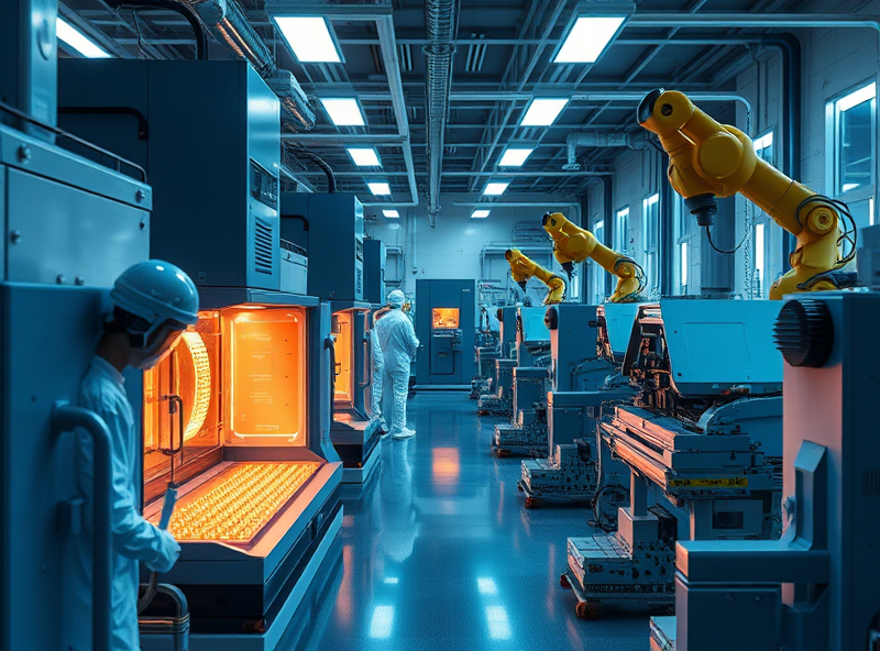
In the fast-paced world of semiconductor innovation, the role of advanced manufacturing technologies is more critical than ever. As chips become smaller, faster, and more energy-efficient, the tools and materials used to create them must evolve in tandem. Applied Materials, a global leader in semiconductor equipment, plays a foundational role in this transformation by providing the ‘pickaxes’—the advanced machinery and materials—that enable chipmakers to push the boundaries of Moore’s Law.
One of the most important technologies driving next-gen chips is Extreme Ultraviolet (EUV) lithography. This method allows chipmakers to etch incredibly fine patterns onto silicon wafers, enabling the production of chips with nodes as small as 3nm and below. Applied Materials supports this process with specialized deposition and etching tools that ensure precision and yield at such tiny scales.
Another game-changing innovation is atomic layer deposition (ALD), which allows for the creation of ultra-thin films one atom at a time. This technique is essential for building 3D transistor architectures like FinFETs and Gate-All-Around (GAA) transistors, which are crucial for maintaining performance gains as traditional scaling slows down.
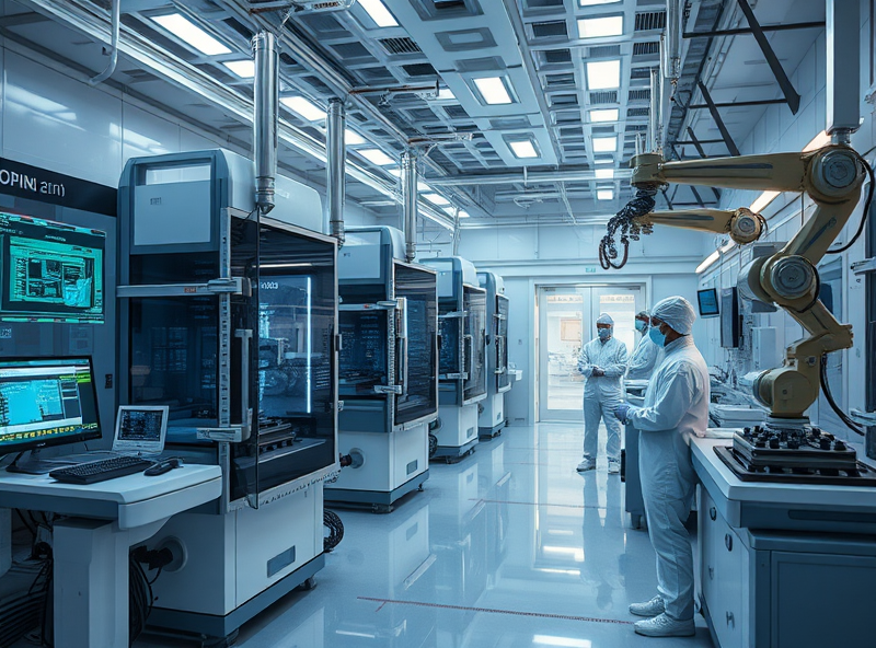
Additionally, advanced metrology and inspection systems are becoming indispensable. These tools help manufacturers detect and correct defects at the atomic level, ensuring higher yields and reliability in production. Applied Materials’ investment in AI-powered process control systems is also helping fabs make real-time adjustments, reducing waste and improving efficiency.
These innovations not only power your smartphone or laptop but also enable advancements in AI, autonomous vehicles, and cloud computing. By understanding the technologies behind chipmaking, we gain a deeper appreciation for the invisible infrastructure that supports our digital lives.
For more on how Applied Materials is shaping the future of semiconductors, you can visit their official newsroom: https://www.appliedmaterials.com/us/en/news.html
Strategic Global Expansion and Ecosystem Collaboration

As the semiconductor industry continues to power global digital transformation, Applied Materials stands out not only for its cutting-edge chipmaking technologies but also for its strategic global expansion and ecosystem collaboration. These efforts are not just about business growth—they’re about building a resilient, innovative, and sustainable semiconductor supply chain that benefits industries and consumers worldwide.
Applied Materials has strategically expanded its presence in key semiconductor hubs such as the United States, Taiwan, South Korea, and Europe. This global footprint allows the company to stay close to its customers, adapt quickly to regional market demands, and ensure supply chain resilience. For example, its new R&D centers and manufacturing facilities in the U.S. and Asia are designed to accelerate innovation while reducing lead times and logistics costs.
Equally important is Applied’s focus on ecosystem collaboration. The company actively partners with chipmakers, equipment suppliers, universities, and government agencies to co-develop next-generation technologies. These collaborations foster open innovation, accelerate time-to-market, and help address industry-wide challenges such as scaling EUV lithography or developing advanced packaging solutions.
This approach not only strengthens Applied Materials’ market leadership but also supports the broader semiconductor ecosystem, ensuring that innovation continues to thrive in a globally interconnected world. For more insights into how ecosystem collaboration is shaping the future of semiconductors, you can refer to this official report by the Semiconductor Industry Association: https://www.semiconductors.org/semiconductors-101/innovation/
By aligning global expansion with deep ecosystem partnerships, Applied Materials is not just enabling the future of chipmaking—it’s helping to build a smarter, more connected world.
Sustainability and Future-Proof Innovation in Chipmaking
As the semiconductor industry continues to evolve at a breakneck pace, sustainability and long-term innovation have become more than just buzzwords—they are now essential pillars for future growth. Applied Materials, a global leader in materials engineering solutions, plays a crucial role in driving eco-conscious innovation in chipmaking.
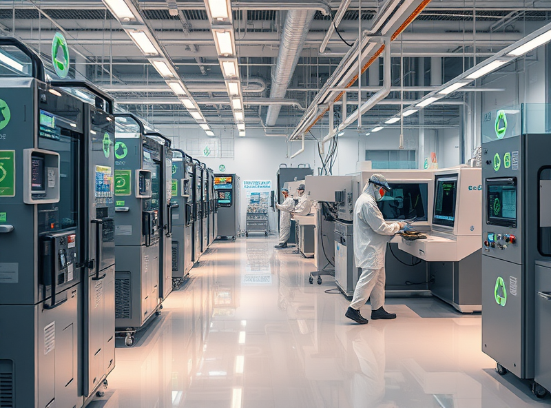
The chip manufacturing process is resource-intensive, involving high energy consumption, use of rare materials, and complex supply chains. To address these challenges, companies like Applied Materials are investing in greener technologies. For instance, they are developing advanced deposition and etching systems that reduce material waste and energy usage. These innovations not only lower environmental impact but also cut operational costs for chipmakers, making sustainability a win-win strategy.
Moreover, Applied Materials is actively collaborating with industry partners to create circular economy models—recycling and reusing materials within the semiconductor ecosystem. This helps reduce dependency on scarce resources and minimizes electronic waste.
Future-proofing chipmaking also means designing tools and processes that can adapt to next-generation nodes and new materials. Applied Materials’ innovations in atomic-level precision and AI-driven process control are helping fabs meet the demands of 2nm and beyond, ensuring that today’s investments remain relevant tomorrow.
By aligning technological advancement with environmental responsibility, Applied Materials is not only shaping the future of semiconductors but also setting a benchmark for sustainable innovation.
For more insights, you can explore Applied Materials’ sustainability initiatives here: https://www.appliedmaterials.com/us/en/sustainability.html